
PCB Manufacturers can inspect to IPC-A-600G and assemble to IPC-A-610 however in order for your PCB design to pass, IPC standards should be implemented from the very beginning of the PCB design from padstacks and footprints through to manufacturing.
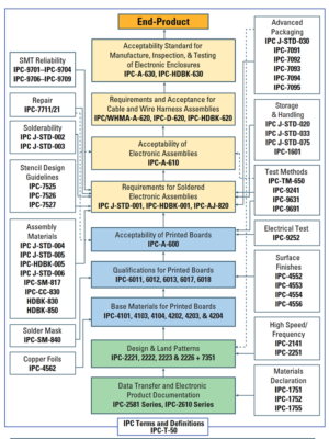
A good starting point for PCB Design is the IPC-2221 and IPC-2222 documents, these form the generic base for PCB layout.
The document IPC 7351, has the guidelines for creating the correct footprints for components used in the PCB layout, with land patterns that are optimised to meet the criteria for solder joint reliability to IPC-J-STD-001.
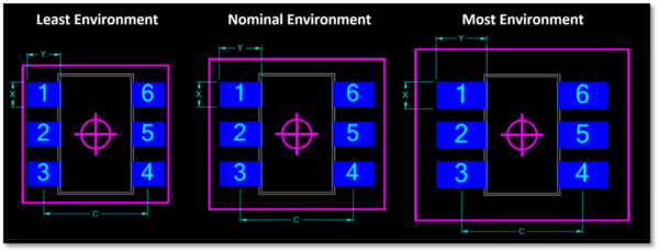
There are three variations for land pattern geometry, these are categorized according to the density of the PCB. “Nominal” is more commonly used rather than “Most” as this geometry has the best performance.
- M – Maximum (Most) Material Condition (Density Level A)
- N – Median (Nominal) Material Condition (Density Level B)
- L – Minimum (Least) Material Condition (Density Level C)
Incorporating IPC 7351 Complaint Electronic Component Information Providers into your CAD system is a quick method to ensure your land patterns and naming conventions match the standard.
PCB designers need to address possible fabrication issues during the design process. This will prevent a redesign as when land patterns are not optimized to IPC standards, this can cause manufacturing defects.
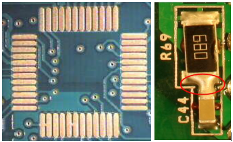
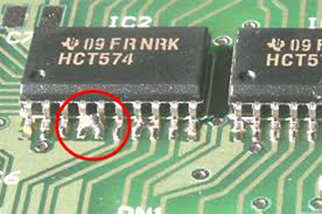
Solder Bridging (Shorts)
Bridging is caused by inadequate spacing or lack of solder resist dams between pads. The courtyard dimensions are also important to ensure the required spacing around the component, too small and this could create shorts because the components are too close together or cause issues with the Pick and Place process. Land patterns should be designed with the dimensions shown in the IPC-7351 standards to ensure the correct heal, fillet and toe dimensions, whilst minimising movement of the component during reflow.
Tombstone phenomenon & Component skewing.
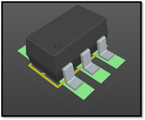
Another issue to consider is the amount of solder paste deposited on the pads and the size of the pads. For example; If the pads are too large, asymmetric or if one pad is larger than the other then this can cause the two solder joints to fail to melt at the same time (different wetting speeds), which can cause component skewing and tombstoning and is most common in 2 pin passive components. Careful consideration of heat dissipation during the PCB design process is required to ensure that the wetting process is completed at the same time. This is easily controlled with today’s convection reflow ovens and the correct pre-heating cycles and cooling cycles.

For PTH components are many factors to consider during the design process that can cause issues due to excessive heat dissipation: during the soldering process. Today’s boards are a mixture of technologies, so the majority of PTH soldering is done using selective soldering. Unlike the old wave method, there is a small fountain of solder, this has less thermal mass than a wave, so excessive thermal dissipation will cause heat to be lost leading to incorrect barrel filling and excessive solder on the pad.
Consider the following during the PCB design process:
- Plated through holes that are too close to the pads, manufacturers’ minimum solder dam and solder mask to pad clearance should be used to ensure the solder doesn’t flow down the PTH.
- When vias in pads are required due to thermal relief, these vias should be plugged according to IPC-4761.
- A pad which has multiple routes connected to it will dissipate heat quicker than a pad which only has one route connected to it.
- Pads connected to Power or Ground can have larger track width rule stacks, if one of the pads has a larger track width then this can cause an imbalance of heat dissipation.
- Large copper planes act like heatsinks so the thermal relief settings of the pad should be carefully considered when routing.
The importance of good library management is often overlooked, it is common that PCB Design Engineers do not realise that manufacturing defects are caused by land patterns that are not optimized to IPC standards. For more information on how to enhance your PCB design skills for manufacture click the link below: